Thick Film Solutions
Ultra Thick film Printed Cu substrate(TPC)
Product Details
Features
-
- Max. film thickness: 0.8mmt, Min. pattern spacing: 0.3mm
- It can be used with silicon nitride, aluminum nitride, sapphire, alumina, etc.
- It has equivalent reliability to the AMB substrate.
Structure
-
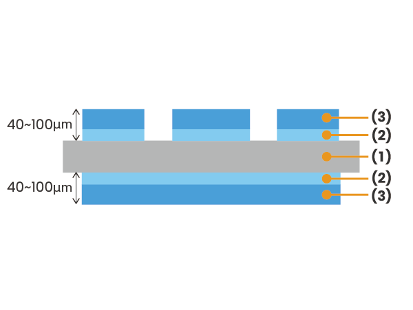
Structure
(1) Substrate
(2) Active metal bonding layer
(3) Copper layer -
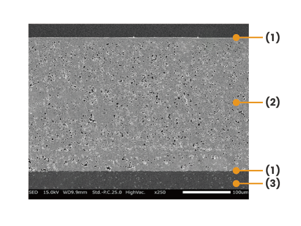
Cross-sectional SEM image
Copper paste ultra-thick film (300μm) fired substrate bonding surface using active metal paste.
(1) Bonding layer
(2) Copper film
(3) AlN substrate
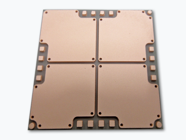
Application Example
-
Ceramic heat-dissipating circuit packages for power devices
Specification
| Item | Reference standard | Remarks | |
|---|---|---|---|
| Base material | Material | AlN, Al₂O₃, SiN | Please contact us for other materials. |
| Size | 50~114mm□ | - | |
| Thickness | 0.2mm~ | - | |
| Conductor properties | L/S | ≧200/200μ | - |
| Film thickness | 100~500μ | For 500µm or more, please contact us. | |
| Resistivity | 2.5~4.0μΩ㎝ | - | |
| Adhesion before plating | ≧3.0kgf/2mm□ | Measured by peel test | |
| Adhesion after plating | ≧2.5kgf/2mm□ | ||
| Durability after plating | Al₂O₃: Thermal shock test, Endurance over 2,000 cycles | 1cycle:-45°C(30min)⇔120°C(30min) | |
| AlN: Thermal shock test, Endurance over 1,500 cycles | 1cycle:-45°C(30min)⇔120°C(30min) | ||
| SiN: Thermal shock test, Endurance over 3,000 cycles | 1cycle:-45°C(30min)⇔150°C(30min) | ||